Nvidia says it’s unlocked a way for the tech industry to produce next-generation chips at a faster rate with less energy costs.
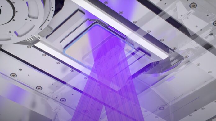
The GPU maker has developed a way to streamline a key part of the chip-making process known as lithography, Nvidia CEO Jensen Huang announced at the company’s GTC event. Lithography essentially involves using light to create the intricate patterns on a silicon wafer to form the microscopic transistors.
Chip makers such as TSMC and Intel use expensive lithography machines to project the light through a “photomask” or “reticle,” which can stencil out the pattern on the silicon wafer. To print the patterns at nano-meter levels, semiconductor makers have to rely on what’s called computational lithography(Opens in a new window)—or specialized computer models—to optimize the photomask and prevent defects during the manufacturing process.
How the lithography works.
(Credit: Nvidia )
The problem is that computational lithography requires extensive calculations and data processing; Jensen called it the “largest computational workload in chip design and manufacturing.” Hence, massive data centers are needed, forcing chip manufacturers to spend big on the computing resources and electricity.
In response, Nvidia is introducing “cuLitho,” a software library the company says can speed up computational lithography up to 40 times. As an example, Jensen noted a single reticle for an Nvidia H100 enterprise GPU could take two weeks to process using existing CPU-based approaches. With cuLitho, a chip maker would only need a single eight-hour shift.
In another example, Jensen added: “TSMC can reduce their 40,000 CPU servers used for computational lithography by accelerating with cuLitho on just 500 DGX H100 systems.”
This would also reduce TSMC’s computational lithography power requirements from 35 megawatts to only 5 megawatts. In addition, cuLitho promises to help manufacturers cut down on the prototyping period to build chips while aiding them in reaching processor designs at 2 nanometers and below.
Recommended by Our Editors
Nvidia spent four years developing cuLitho, which runs on the company’s enterprise GPU hardware. TSMC, which makes chips for both Nvidia and Apple, plans on “qualifying” cuLitho for production starting in June, Jensen added. ASML, a maker of lithography machines, is also working with the company on integrating cuLitho into its products in the future.
“In the near term, fabs using cuLitho could help produce each day 3 to 5x more photomasks—the templates for a chip’s design—using 9x less power than current configurations,” Nvidia added. “Longer term, cuLitho will enable better design rules, higher density, higher yields and AI-powered lithography.”
Get Our Best Stories!
Sign up for What’s New Now to get our top stories delivered to your inbox every morning.
This newsletter may contain advertising, deals, or affiliate links. Subscribing to a newsletter indicates your consent to our Terms of Use and Privacy Policy. You may unsubscribe from the newsletters at any time.
Hits: 0


